Introduction
In the previous article, I designed an analog front-end (AFE) board for reading PT100 signals using an ADC instead of the dedicated MAX31865 IC, and verified that the amplification stage worked properly.
See the AFE design for PT100 temperature measurement
PT100 Temperature Measurement AFE (Analog Front End) Design
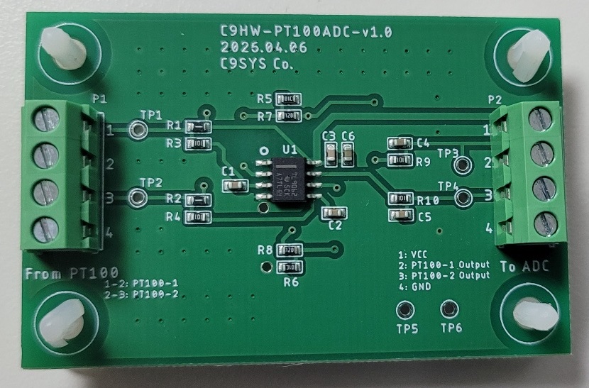
Below is the actual fabricated C9HW-PT100ADC-v1.0 board.
In this article, I will use this board and read its analog output voltage directly through the ADC of the STM32F103.
Instead of connecting an actual PT100 sensor, two fixed resistors were connected to compare the ADC measurement results with actual voltage measurements.
In other words, this experiment is intended to verify how accurately the STM32 ADC can read real analog signals.
Experiment
Preparation
The following equipment was used for this experiment:
- PT100 Analog Front-End Board (AFE) – self-designed
- STM32F103 development board – purchased from AliExpress
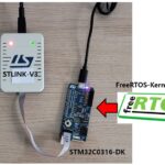
- Debugger (ST-LINK V2 or V3) – in this experiment, the built-in debugger of the NUCLEO-F429ZI board was used
- Two fixed resistors (99Ω and 149.3Ω)
- Multimeter
- Development environment: STM32CubeIDE
Experiment Setup
The experiment setup was completed using the above equipment.
The actual connection setup was photographed to clearly show each component and their relationship.
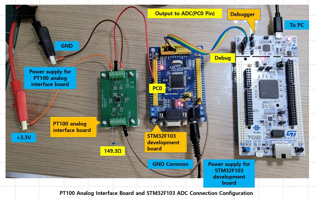
In this experiment, a fixed resistor of 149.3Ω was connected instead of the PT100 sensor to check the output characteristics of the analog interface board.
For comparison, another resistor of 99Ω (used as a substitute for 100Ω) was also prepared and tested alternately.
The 100Ω resistor represents the resistance value of a PT100 sensor at 0°C.
Therefore, by using these two resistors, it is possible to indirectly verify how the output voltage changes according to temperature variation.
The board was powered with 3.3V, and the output signal was connected directly to PC0 (ADC1_IN10) of the STM32F103.
For stable measurement, the GND of the analog interface board and the STM32F103 board were connected together (common ground).
This is very important because it ensures that both the analog board output voltage and the STM32 ADC input voltage share the same reference level.
ADC Configuration
The following shows how to configure the ADC in the STM32F103.
To use the ADC, several parameters must be configured.
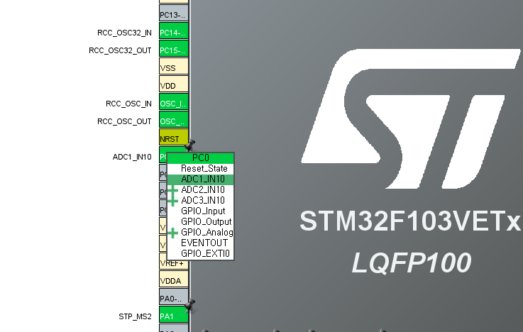
First, the ADC input pin must be selected.
In this experiment, PC0 was used as the ADC input pin, which corresponds to ADC1_IN10.
This configuration can be easily done in CubeMX within STM32CubeIDE.
Below is the configuration screen where PC0 was set as ADC1_IN10.
Next, various ADC parameters need to be configured.
In CubeMX, go to:
Pinout & Configuration → Analog → ADC1
The Mode section does not require additional settings because it is configured automatically when the input pin is assigned.
The important part is the Configuration section.
In this experiment, the ADC was configured in:
- Single Channel Mode
- Single Conversion Mode
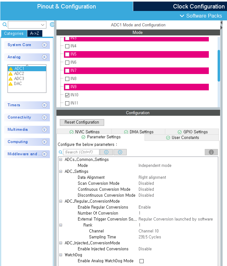
The settings were configured as follows:
- Data Alignment: Right Alignment
- Scan Conversion Mode: Disabled
- Continuous Conversion Mode: Disabled
- External Trigger: Software Start
- Regular Channel: ADC1_IN10 (PC0)
The sampling time was initially set to 1.5 cycles, but the measurement was unstable.
For stable measurement, it was changed to 239.5 cycles.
Finally, the ADC clock must be configured.
This setting can be found in the Clock Configuration tab of CubeMX.
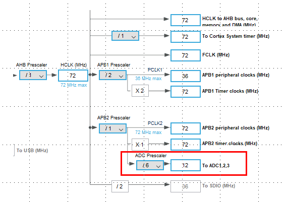
In this experiment:
- System Clock = 72MHz
- ADC Prescaler = /6
- ADC Clock = 12MHz
If the ADC clock is too high, measurement errors may increase.
Generally, setting the ADC clock around 12MHz provides stable operation.
After configuring the clock settings, the ADC setup is complete.
Saving the project will automatically generate the initialization code.
Firmware Implementation
Now that the ADC configuration is complete, the next step is firmware implementation.
To improve maintainability and scalability, the ADC-related code was separated into dedicated header and source files.
- Header file: pt100_adc.h
- Source file: pt100_adc.c
Header File(pt100_adc.h)
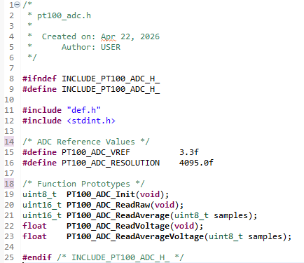
The header file defines:
- ADC function prototypes
- Reference voltage constants
- ADC resolution constants
Here:
- PT100_ADC_VREF represents the ADC reference voltage
- PT100_ADC_RESOLUTION represents the maximum value of a 12-bit ADC (4095)
The header file acts as an interface for external modules to use the ADC functions.
Source File(pt100_adc.c)
The source file implements the actual ADC functionality.
Initialization Function
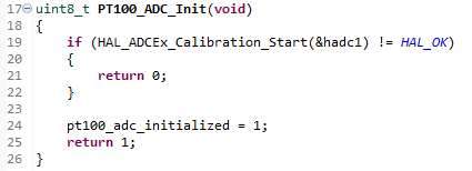
This function performs ADC calibration.
On STM32F103 devices, ADC calibration before measurement is recommended for improved accuracy.
After successful calibration, an internal flag is set so the ADC reading functions can operate.
Reading a Single ADC Value
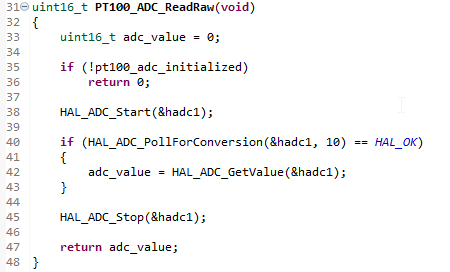
This function starts the ADC once, waits until conversion is complete, and returns the converted value.
Since this experiment uses the polling method, the conversion completion is checked using:
HAL_ADC_PollForConversion()
This is the most basic single-sample ADC reading method.
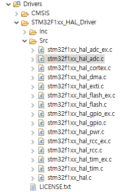
The ADC-related functions provided by the HAL library can be found in the Drivers → STM32F1xx_HAL_Driver → Src folder within the Project Explorer.
Averaging ADC Values
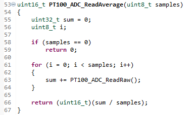
ADC values may fluctuate slightly depending on the measurement moment.
Therefore, averaging multiple samples is more stable than using a single reading.
This function reads ADC values multiple times and returns the average.
In this experiment, 16 samples were used.
This acts as a simple software filter to reduce noise.
Voltage Conversion
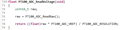
This function converts the raw ADC value into an actual voltage.
Since STM32F103 uses a 12-bit ADC, the raw value ranges from 0 to 4095.
The actual voltage is calculated based on the 3.3V reference.
This is necessary to compare ADC results with multimeter measurements.
Average Voltage Calculation
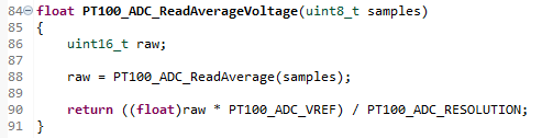
This function converts the averaged ADC value into voltage.
This method provides more stable voltage values.
In actual applications, it is more efficient to first calculate the average ADC value and then convert it into voltage.
Application Integration
In this project, the overall functionality is managed by app.h and app.c.
Before using the ADC, initialization must be performed.
The initialization function:
PT100_ADC_Init()
was called in:
appInit()
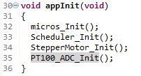
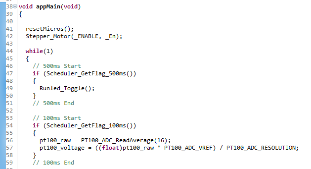
The actual ADC reading operation was executed in the 100ms periodic task inside appMain().
Since temperature changes relatively slowly, a 100ms sampling interval is sufficient for stable measurement.
Using:
PT100_ADC_ReadAverage(16)
16 samples were averaged and converted into voltage.
ADC Reading Experiment
After completing the firmware implementation, the project was built and downloaded in Debug mode.
To monitor ADC values in real-time:
- pt100_raw
- pt100_voltage
were added to Live Expressions.
By pressing Resume, the variables can be monitored in real-time without stopping the program.
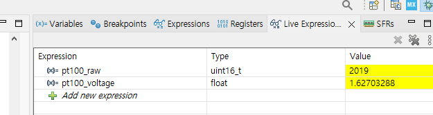
The results above were measured with a 99.3Ω resistor connected to the system.
Using the Live Expression feature allows you to monitor variable values in real time without stopping the program, making it highly effective for debugging and validating measurements.
Using the same method, both resistors (99.3Ω and 149.3Ω) were tested, and the following values were recorded.
| Condition | Resistance (Ω) | Input Voltage (V) | Board Output (V) | ADC Raw | ADC Voltage (V) |
|---|---|---|---|---|---|
| Reference 1 | 99.3 | 0.1153 | 1.614 | 2019 | 1.627 |
| Reference 2 | 149.3 | 0.17 | 2.39 | 2990 | 2.40 |
| Open | ∞ | – | 3.3 | 4095 | 3.29 |
For both 99.3Ω and 149.3Ω, the ADC voltage values were very close to the actual board output voltage.
It was also confirmed that as resistance increased, both the output voltage and ADC raw value increased linearly.
In the open condition, the ADC raw value reached 4095, confirming full-scale saturation.
This verifies that the STM32F103 ADC can correctly read the analog output of the PT100 interface board.
Conclusion
In this experiment, I directly measured the output voltage of the analog interface board using the STM32F103 ADC and compared it with actual voltage measurements.
Using fixed resistors (99.3Ω and 149.3Ω), it was confirmed that the converted ADC voltage closely matched the actual board output voltage.
It was also verified that the output voltage and ADC values increased linearly as resistance increased.
In the open condition, the ADC reached its maximum value, confirming normal operation.
This experiment also showed that hardware factors such as:
- Sampling Time
- ADC Clock
- Common Ground Configuration
have a significant impact on measurement accuracy.
This demonstrates that the STM32F103 ADC, when used with a proper analog front-end circuit, can provide practical and reliable PT100 measurements even without a dedicated interface IC.
PT100 Temperature Measurement Series
PT100 temperature measurement series organized step-by-step from Analog Front End design to STM32 ADC Polling, Time-Distributed Sampling, ADC DMA implementation, and 3-wire PT100 constant current drive design.
Part 1: AFE (Analog Front End) Design for PT100 Temperature Measurement
PT100 Temperature Measurement AFE (Analog Front End) Design
Part 2: Reading PT100 Signals Using STM32F103 ADC (Polling Method)
Part 3: STM32 ADC Time-Distributed Sampling Design Method
STM32 ADC Time-Distributed Sampling Design Method
Part 4: Implementing PT100 Temperature Measurement Using STM32 ADC DMA
Implementing PT100 Temperature Measurement Using STM32 ADC DMA
Part 5: 3-Wire PT100 Constant Current Driven AFE Design (TLV9062 + INA826)
3-Wire PT100 Constant Current Driven AFE Design(TLV9062+INA826)


“Reading PT100 Signals with STM32F103 ADC (Polling Method Experiment)”에 대한 3개의 생각