Overview
There are many types of sensors for temperature measurement, but selecting a sensor that can operate reliably in real industrial environments is not always easy.
In general, temperature sensors can be divided into two major categories: NTC thermistors and PT100 RTD sensors.
NTC sensors have the characteristic that resistance decreases as temperature increases. However, the resistance change is nonlinear, requiring compensation or a lookup table for MCU processing. Their precision is also relatively lower.
On the other hand, PT100 sensors have a resistance of 100Ω at 0°C, and their resistance changes relatively linearly with temperature. Because of this, they are widely used in applications requiring high precision temperature measurement. However, since the resistance variation is very small, signal amplification is required before measurement.
To solve this problem, dedicated RTD interface ICs are commonly used. One representative example is the Analog Devices MAX31865, which provides an easy SPI-based interface to the MCU.
I have also used the MAX31865 in several projects without major issues under normal operating conditions. However, in a recent project, stepper motors, DC motors, solenoid valves, and AC heaters were operating simultaneously, creating significant electrical noise.
In such an environment, the MAX31865 occasionally generated fault conditions, causing temperature measurement interruptions. Even though the sensor itself was normal, intermittent measurement failures could critically affect the control system.
To solve this problem, I decided to directly amplify the small analog voltage generated by the PT100 sensor using an op-amp and measure it through the MCU ADC without using a dedicated RTD IC.
In this article, I summarize the design and PCB implementation process of an AFE for PT100 temperature measurement.
Circuit Design
Design Concept
To directly measure a PT100 using the MCU ADC without a dedicated IC, the following conditions must be satisfied:
- Limit the sensor current to minimize self-heating
- Amplify the small μV–mV level signal stably
- Filter noise to maintain stable operation in noisy environments
To achieve this, the following signal chain was selected:
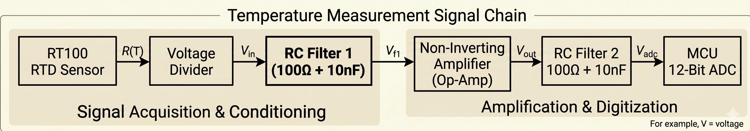
The small voltage generated by the PT100 passes through filtering and amplification, expanding the input range so that the MCU ADC can process it effectively.
Reference Resistor(RREF) Selection
The excitation current flowing through the PT100 is very important.
If the sensor current increases, self-heating caused by I²R power dissipation increases, resulting in measurement errors.
In practical applications, approximately 1mA is commonly used as a compromise between signal level and self-heating.
In this design:
The excitation current is calculated as:
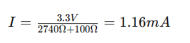
So approximately 1.16mA flows through the PT100.
This is an appropriate level for temperature measurement.
If a much smaller resistor such as 100Ω were used, the current would increase to tens of mA, causing severe self-heating and making accurate measurement impossible.
PT100 Connection Method(2-Wire)
In this design, the PT100 is connected using a 2-wire configuration.
Since lead-wire resistance was relatively small compared to system noise, simplicity and stability were prioritized.
PT100 sensors generally support:
- 2-wire
- 3-wire
- 4-wire
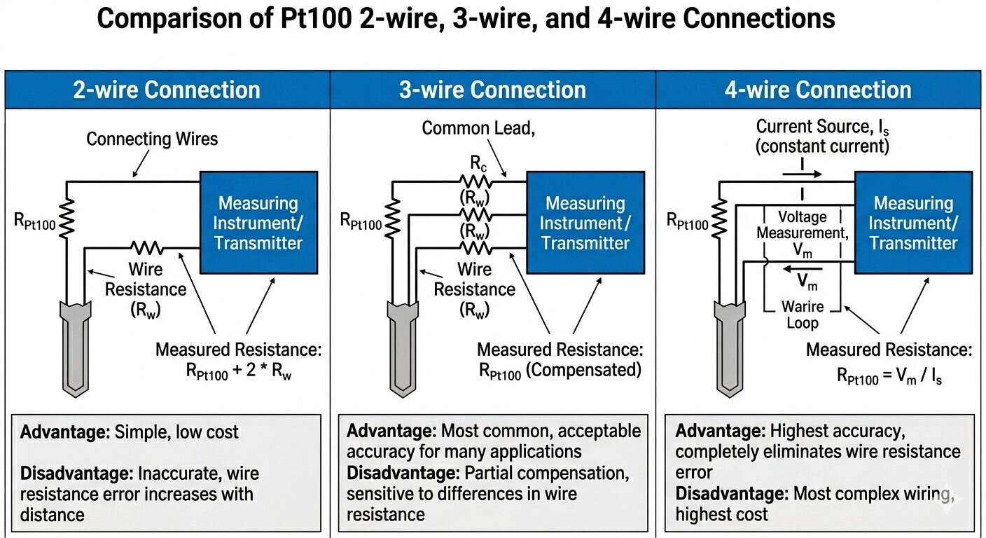
The 2-wire method is the simplest, but the lead resistance is included in the measured value.
This design adopted the 2-wire method for the following reasons:
- Short cable distance
- Very small lead resistance
- Simpler circuit structure
Considering the target temperature range (0°C–200°C) and required precision, the 2-wire method provides sufficient practical performance.
For higher accuracy or longer sensor cables, 3-wire or 4-wire configurations may be required.
Input Voltage Range
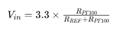
The PT100 resistance changes with temperature, generating the following input voltages:
| Temperature | Resistance | Input Voltage |
|---|---|---|
| 0°C | 100Ω | 0.116V |
| 150°C | 157Ω | 0.179V |
| 200°C | 176Ω | 0.199V |
The input signal is very small (approximately 0.1V–0.2V), making it difficult to fully utilize the MCU ADC input range (0–3.3V).
Therefore, amplification is necessary.
The input voltage can be expressed as:
OP-Amp Gain Design
A non-inverting amplifier was used.
The gain equation is:
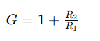
R1 = 10kΩ
R2 = 130kΩ
Therefore:
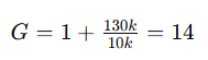
This gain expands the input signal into a range suitable for the MCU ADC.
The op-amp used is:
TLV9062
You can download the datasheet of TLV9062 at the link below:
TLV9062 Datasheet Download
Output Voltage Range
With a gain of 14:
| Temperature | Input Voltage | Output Voltage |
|---|---|---|
| 0°C | 0.116V | 1.62V |
| 150°C | 0.179V | 2.50V |
| 200°C | 0.199V | 2.78V |
This output range fits safely within the MCU ADC input range (0–3.3V), leaving enough headroom to avoid saturation.
RC Filter Design
Since the PT100 signal is very small, proper filtering is necessary.
This design applies RC filtering at both input and output:
Input Filter: 100Ω + 10nF
Output Filter: 100Ω + 10nF
The cutoff frequency is:
![]()
Substituting the values:
![]()
So high-frequency noise above approximately 159kHz begins to attenuate.
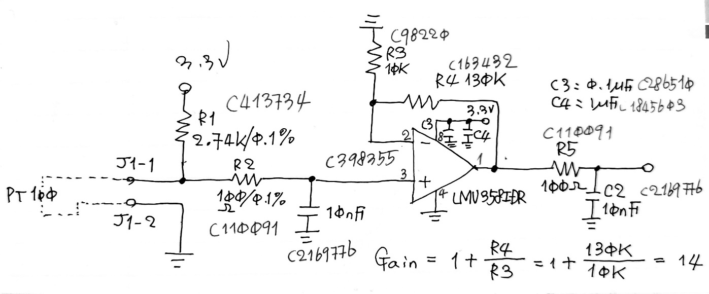
Based on the design specifications mentioned above, I have developed the following circuit configuration. This is a hand-written draft from the initial design phase, used to quickly review the overall architecture and determine key parameters.
PCB Design
Schematic Design
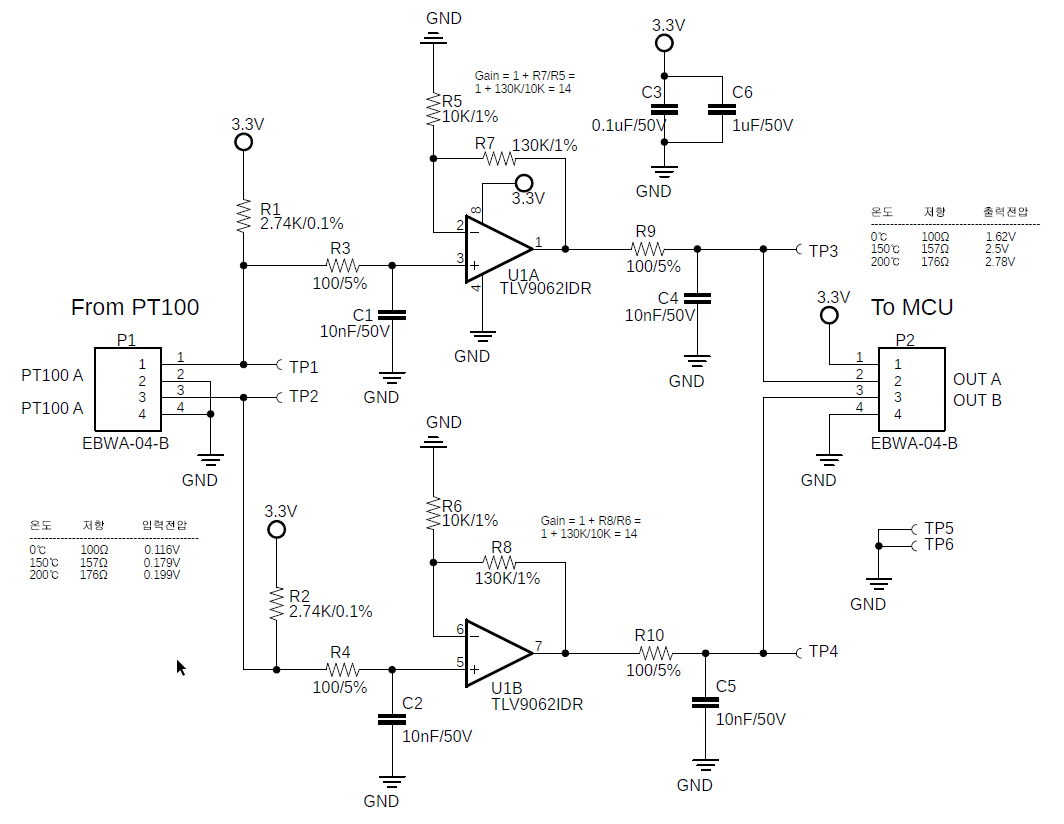
Based on the design parameters above, the schematic was created.
The originally planned LM358 was replaced by the TLV9062 because it was readily available in the JLCPCB SMT assembly service through LCSC.
The circuit accepts dual PT100 inputs and amplifies them independently before sending them to the MCU ADC.
Both channels use the same structure for stable temperature comparison.
Shown below is the full circuit diagram for the system.
PCB Layout Design
Shown below is the finalized PCB layout and 3D rendering of the board.
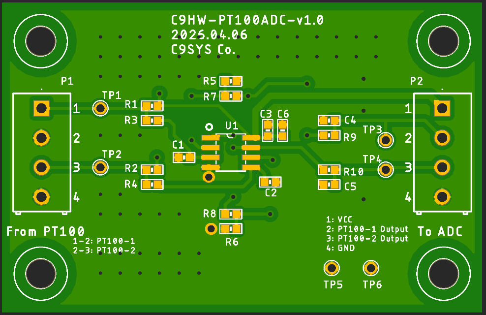
The PCB layout was designed considering analog signal characteristics:
- Minimized input signal routing length
- Physical separation of input and output traces
- Ground plane optimization
- Via stitching for stable return paths
- Decoupling capacitors near the op-amp
Because the PT100 signal is at the millivolt level, minimizing noise coupling was an important design priority.
Conclusion
In this article, I described the design process of an AFE for PT100 temperature measurement without using a dedicated RTD interface IC.
Previously, dedicated ICs such as the MAX31865 allowed relatively simple temperature measurement implementation. However, in noisy industrial environments, intermittent faults made stable operation difficult.
To solve this, the following approach was used:
- Apply approximately 1mA excitation current to minimize self-heating
- Generate a small voltage through a resistor divider
- Amplify the signal into the ADC input range
- Apply RC filtering to reduce noise
- Improve signal stability through PCB layout optimization
Through this structure, it was confirmed that stable temperature measurement is possible without a dedicated RTD IC.
In industrial environments where electrical noise is severe, this analog-based approach can be a more robust and stable solution.
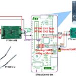
PT100 Temperature Measurement Series
PT100 temperature measurement series organized step-by-step from Analog Front End design to STM32 ADC Polling, Time-Distributed Sampling, ADC DMA implementation, and 3-wire PT100 constant current drive design.
Part 1: AFE (Analog Front End) Design for PT100 Temperature Measurement
Part 2: Reading PT100 Signals Using STM32F103 ADC (Polling Method)
Reading PT100 Signals with STM32F103 ADC (Polling Method Experiment)
Part 3: STM32 ADC Time-Distributed Sampling Design Method
STM32 ADC Time-Distributed Sampling Design Method
Part 4: Implementing PT100 Temperature Measurement Using STM32 ADC DMA
Implementing PT100 Temperature Measurement Using STM32 ADC DMA
Part 5: 3-Wire PT100 Constant Current Driven AFE Design (TLV9062 + INA826)
3-Wire PT100 Constant Current Driven AFE Design(TLV9062+INA826)


“PT100 Temperature Measurement AFE (Analog Front End) Design”에 대한 4개의 생각