Introduction
So far, we have covered several approaches for designing an Analog Front End (AFE) to directly read PT100 temperature sensors using an STM32 ADC.
Instead of using dedicated RTD interface ICs such as MAX31865, the previous approach used a simple voltage divider circuit and an amplifier to convert PT100 resistance changes into voltage.
This method has the advantage of a simple circuit structure, low component cost, and direct implementation using the MCU’s ADC.
However, since the PT100 itself is a low-resistance sensor, the resistance of the lead wires directly affects the measured voltage, which limits precision.
In addition, because the voltage-divider structure inherently depends on supply voltage variations, there are limitations in long-term stability.
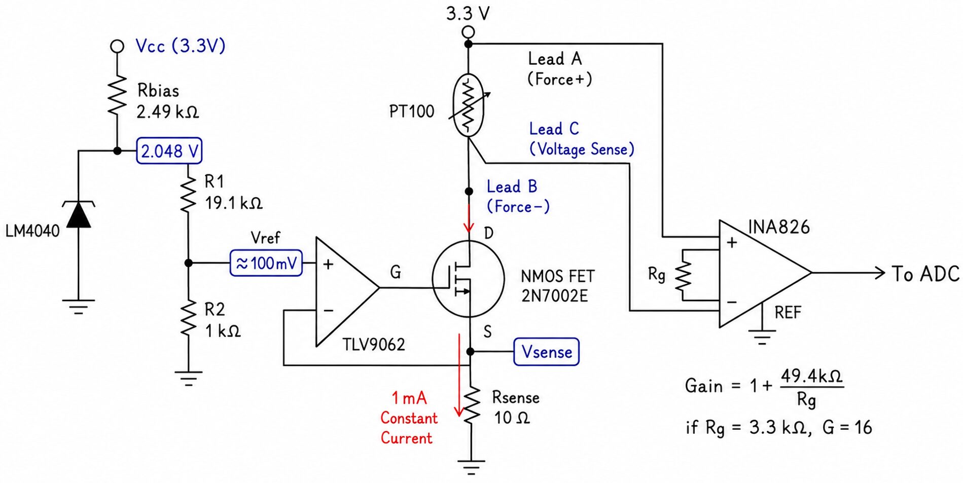
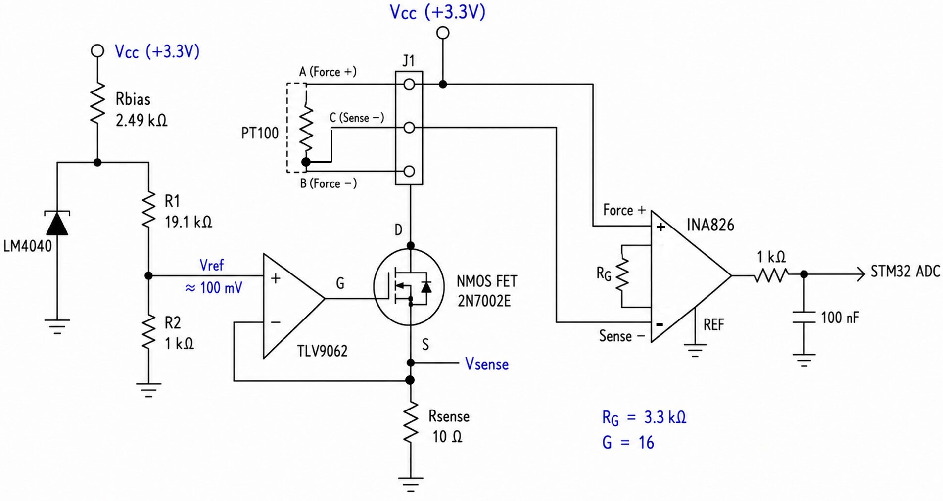
In this article, to overcome these limitations, we will design a 3-wire PT100-based constant current driven AFE.
By driving a constant current through the PT100, the sensor voltage becomes directly proportional to resistance, and by adopting a 3-wire structure, lead-wire resistance errors can be reduced.
Additionally, by combining a general-purpose Op-Amp with an Instrumentation Amplifier, we will build a more stable and precise temperature measurement circuit.
Why 3-Wire PT100?
Limitations of 2-Wire Configuration
The 2-wire PT100 configuration is the simplest structure.
Since only two wires are required to connect the sensor, circuit implementation is simple and wiring cost is low.
For compact equipment or low-cost systems, this method is still widely used.
However, because PT100 resistance variation is very small, lead-wire resistance directly affects the measurement result.
The nominal resistance of PT100 is 100Ω at 0°C, and the resistance change is approximately:
![]()
This means that even an additional 0.385Ω of lead resistance can cause about 1°C error.
For example:
- Lead wire 1 = 0.5Ω
- PT100 = 100Ω
- Lead wire 2 = 0.5Ω
Then:
![]()
That means an additional 1Ω is included.
Converted into temperature:
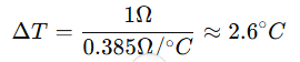
This results in approximately 2.6°C error.
Such errors become relatively larger at lower temperatures and are affected by cable length and contact resistance.
PT100 measurement usually works by applying a constant current and measuring the resulting small voltage.
For example, with 1mA excitation at 0°C:
![]()
At this low signal level, lead resistance, noise, and contact quality have a significant impact.
As a result, while the 2-wire structure is simple and easy to implement, it has inherent limitations when precision temperature measurement is required.
The practical solution is the 3-wire compensation method.
Principle of 3-Wire Compansation
The biggest problem in a 2-wire PT100 configuration is that lead resistance is directly included in the measurement.
To solve this problem, the industrial standard solution is the 3-wire PT100 configuration.
The PT100 is connected using three wires.
At first glance, it may look like just one additional wire, but the measurement principle is fundamentally different.
The core idea is separating:
- Force Path (current path)
- Sense Path (voltage measurement path)
In the diagram:
- Red line → current path
- Blue line → voltage sensing path
Current flows from Force+ (A) into the PT100 and returns through Force− (B).
Voltage drops caused by lead resistance occur in this current path.
However, the actual measurement is taken between Force+ (A) and Sense (C):
![]()
The important point is that Sense line (C) is connected only to the input of the differential amplifier, which has very high input impedance.
Since the INA826 input current is nearly zero:
![]()
There is virtually no voltage drop across the Sense lead resistance.
Therefore, the measured voltage becomes very close to the actual PT100 terminal voltage.
As a result:
- Reduced lead resistance error
- Maintained precision over long cable distances
- Improved industrial reliability
Although the most ideal method is 4-wire Kelvin measurement, the 3-wire method offers an excellent balance between precision, cost, and complexity.
Design Direction and Overall Structure
Design Goals
The goal of this 3-wire PT100 AFE design is not simply reading PT100 resistance.
The goal is to build a stable Analog Front End capable of precise temperature measurement directly through the STM32 ADC.
Compared to the previous voltage-divider method, this design focuses on:
Stable Constant Current Supply
PT100 is a resistive sensor.
To make the measured voltage accurately proportional to resistance, a stable excitation current is required.
The basic relationship is:
![]()
If current remains constant, PT100 resistance changes directly translate into voltage changes.
In this design, approximately 1mA was chosen.
This current minimizes self-heating while providing sufficient signal voltage.
Lead Resistance Compensation
In industrial applications, sensor-to-controller distance is often long.
Lead resistance cannot be ignored.
By separating Force Path and Sense Path using the 3-wire method, lead resistance influence is minimized.
ADC Input Range Optimization
STM32 ADC input range is typically:
0V ~ 3.3V
Since PT100 generates only tens to hundreds of millivolts, direct ADC input would not fully utilize ADC resolution.
To solve this, a differential amplifier is used.
In this design:
INA826 is used.
Practicality and Component Availability
High-precision RTD circuits often become complex and expensive.
This design uses:
- TLV9062
- INA826
to balance precision, simplicity, and practical availability.
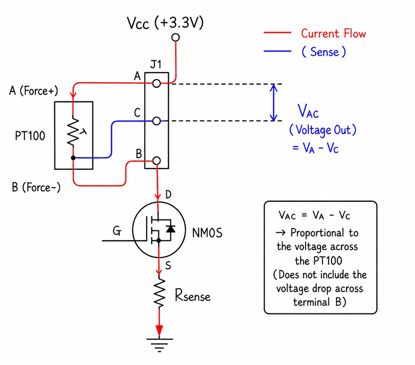
Overall Circuit Structure
The complete circuit consists of five blocks:
- Reference voltage generation
- Constant current source
- 3-wire PT100 sensing
- Differential amplification
- ADC anti-aliasing filter
The operation flow is:
Reference Voltage → Constant Current Source → PT100 → Differential Amplifier → ADC Filter → STM32 ADC
Circuit Design
Reference Voltage Design
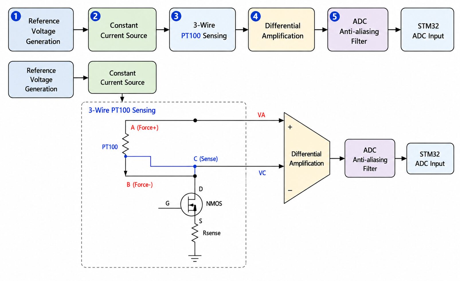
One of the most important elements in a PT100 constant-current drive circuit is a stable reference voltage.
The output current of the constant-current source is determined by the reference voltage, so if the reference voltage fluctuates, the current supplied to the PT100 also changes, directly affecting measurement accuracy.
In this design, the LM4040 was used as the reference voltage device.
The LM4040 is a precision shunt reference that provides stable reference voltage and has low drift over temperature, making it suitable for precision measurement circuits.
The circuit input supply voltage is 3.3V, and operating current is supplied to the LM4040 through the resistor Rbias, generating a stable 2.048V reference voltage.
The current flowing through Rbias is divided into the LM4040 operating current and the load current:
![]()
Where:
- IZ: LM4040 operating current
- IL: Voltage divider load current
The 2.048V reference voltage generated by the LM4040 is then reduced to approximately 100mV through the resistor divider (R1, R2).
The voltage division relationship is:
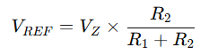
With:
- R1 = 19.1kΩ
- R2 = 1kΩ
The resulting reference voltage:
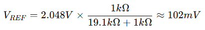
This reference voltage is later used as the input reference for the Op-Amp constant-current block and determines the PT100 excitation current.
For example, if the sensing resistor is configured as 100Ω, the supply current becomes approximately 1mA.
This structure has the advantage that reference generation and current setting are clearly separated, making design changes and calibration easier.
In the next section, we will examine how to generate constant current using this reference voltage with an Op-Amp and MOSFET.
Constant Current Design Using OP-Amp
Once the reference voltage is prepared, the next step is constructing a constant current source that supplies a fixed current to the PT100.
In this design, an Op-Amp + MOSFET current sink structure was used.
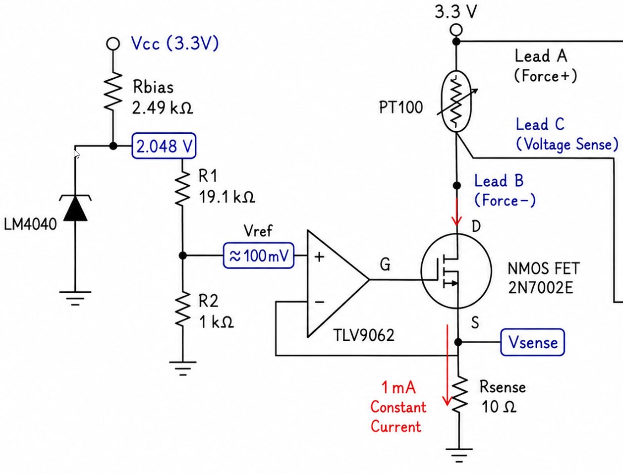
The Op-Amp used here is the TLV9062.
The TLV9062 has rail-to-rail input and output characteristics and can operate stably in a single-supply environment, making it suitable for low-voltage precision measurement circuits.
The operating principle of the constant current source is based on Op-Amp feedback control.
The Op-Amp compares the reference voltage and the voltage across the sensing resistor and adjusts the MOSFET gate voltage.
The important point here is that the MOSFET is not used as a switching device, but rather as a variable resistor operating in the linear region.
From the graph below, it can be seen that the MOSFET drain current changes according to gate voltage, and through Op-Amp feedback control, the desired current is automatically regulated.
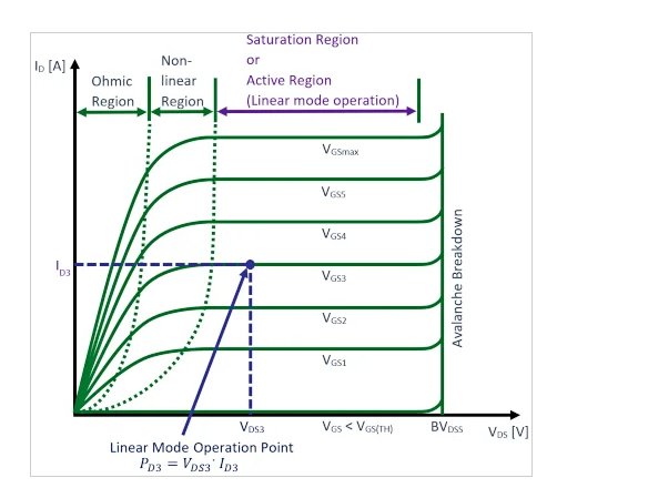
Using this linear operating characteristic, the Op-Amp continuously adjusts the MOSFET gate voltage so that the voltage across the sensing resistor matches the reference voltage.
That is:
![]()
In other words, the Op-Amp automatically controls the MOSFET gate voltage so that the voltage across the sensing resistor Rsense equals the reference voltage.
The current flowing through the sensing resistor is then determined as:
![]()
In this design:
- Vref ≈ 100mV
- Rsense = 100Ω
So:
![]()
This means that approximately 1mA of constant current flows through the PT100.
The biggest advantage of this method is that even if PT100 resistance changes, the current remains nearly constant.
Therefore, the voltage across the PT100 becomes directly proportional to resistance:
![]()
For example, when PT100 = 100Ω:
![]()
As temperature rises, PT100 resistance increases, and the voltage increases proportionally.
Also, by using a MOSFET, the current burden on the Op-Amp output stage can be reduced, resulting in more stable current control.
The constant current source configured this way is combined with the 3-wire PT100 connection structure to form the foundation for more accurate temperature measurement.
If you want to learn more about Op-Amp-based constant current source design principles, you can refer to the material below:
Design a Voltage Controlled Current Source Circuit using Op-Amp
3-Wire PT100 Connection Structure
As explained earlier, the 3-wire PT100 separates the Force Path and Sense Path to reduce measurement error caused by lead resistance.
In this circuit, this principle is applied to the actual circuit so that the voltage across the PT100 can be extracted more accurately.
The PT100 is connected to the circuit through three lead wires:
- Lead wire A (Force+): constant current supply
- Lead wire B (Force−): current return path
- Lead wire C (Sense): voltage sensing line
The 1mA constant current generated by the current source block is supplied to the PT100 through lead wire A and returns to the NMOS current sink circuit through lead wire B.
During this process, a voltage proportional to resistance is generated across the PT100:
![]()
The important point here is the sensing line (C).
The sensing line is connected to the input of the differential amplifier INA826.
Since it has very high input impedance, almost no current flows through it.
Therefore, almost no voltage drop occurs due to lead resistance in the sensing line.
The actual measured voltage consists of the voltage difference between lead wire A and lead wire C:
![]()
This voltage is very close to the actual voltage across the PT100.
The lead resistance voltage drop occurring in the Force− path (B) is excluded from the sensing reference (C), so it does not directly affect measurement.
As a result, PT100 resistance variation can be extracted more accurately, and measurement error can be minimized even in long cable environments.
The extracted low-level PT100 signal is then amplified in the next stage using the differential amplifier INA826 to match the MCU ADC input level.
Differential Amplifier (INA826) Design
The extracted PT100 voltage is a very small signal in the range of several tens to hundreds of millivolts.
If this signal is measured directly by the STM32 ADC, the full ADC input range cannot be effectively utilized, and resolution efficiency is low.
To solve this, this design uses the Instrumentation Amplifier INA826 to amplify the PT100 micro-voltage signal.
The INA826 has high input impedance and excellent common-mode rejection ratio (CMRR), making it suitable for amplifying low-level differential signals.
In this circuit, the voltage difference between Force+ and Sense− is fed into the INA826 input and amplified as a differential signal.
The gain of the INA826 is determined by the external gain resistor RG:
![]()
In this design, the target gain was approximately 16x.
Accordingly, the gain resistor was selected as:
![]()
When 1mA constant current is supplied to PT100, the PT100 voltage at 0°C becomes:
![]()
Amplified by 16 times:
![]()
For example, if temperature rises and PT100 resistance becomes 150Ω:
![]()
Amplified output:
![]()
This allows the PT100 temperature range to be fully utilized within the STM32 ADC input range (0~3.3V).
This improves ADC resolution and allows small temperature changes to be detected more reliably.
ADC Input Filter Design
The amplified output signal from the INA826 is finally delivered to the STM32 ADC input.
At this stage, since the signal is already amplified, if external noise or switching noise is introduced, it directly affects ADC values.
To prevent this, a simple RC low-pass filter is placed before the ADC input to remove high-frequency noise.
In this circuit, a series resistor is inserted between the INA826 output and STM32 ADC input, and a capacitor is connected from the ADC input to GND.
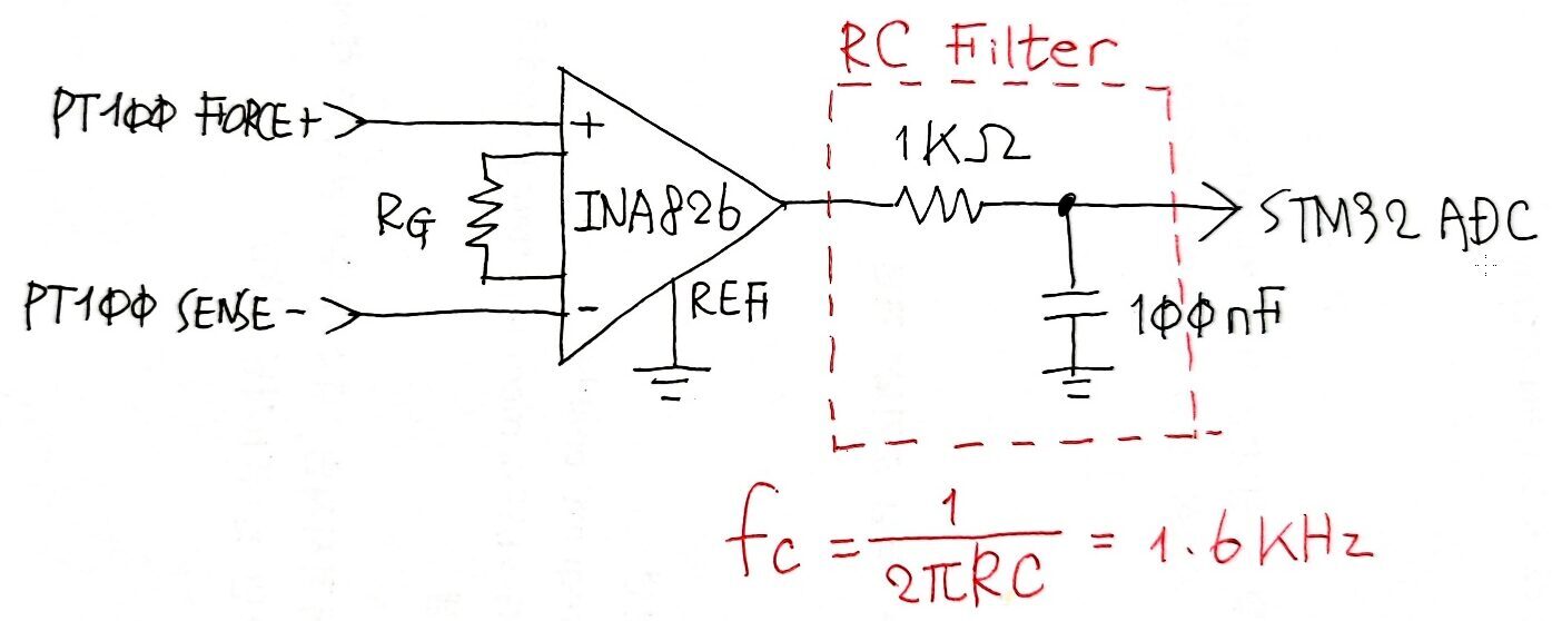
This structure diverts high-frequency components to GND, allowing only a relatively stable low-frequency signal to reach the ADC.
PT100 temperature changes are generally slow signals in the range of several hundred milliseconds or more, so ADC stability and noise rejection are more important than fast response.
The filter cutoff frequency is calculated as:
For example, if:
- Rfilter = 1kΩ
- Cfilter = 100nF
Then:
![]()
That means the cutoff frequency is approximately 1.6kHz.
This level has almost no effect on temperature measurement signals while helping reduce high-frequency noise.
The series resistor also partially serves as ADC input protection.
When external noise or transient voltage changes occur, it can limit direct current flow into the ADC input.
Although the ADC input filter does not change signal amplitude like the amplifier stage, it plays an important role in improving stability and repeatability in real equipment environments.
Complete Circuit Configuration and Expected Analysis
By integrating the reference voltage generation, constant current drive, 3-wire sensing, differential amplification, and ADC filter described above, the complete circuit structure is formed.
The main conditions for calculating expected circuit operation are:
- Constant current: 1mA
- PT100 nominal resistance (0°C): 100Ω
- INA826 gain: 16x
- STM32 ADC reference voltage: 3.3V
- ADC resolution: 12-bit (4096 steps)
Since the current flowing through the PT100 is fixed at 1mA, the PT100 voltage becomes directly proportional to resistance:
![]()
At 0°C:
![]()
Amplified by INA826:
![]()
Converted to STM32 ADC value:
![]()
So:
![]()
When temperature rises and PT100 resistance increases:
For example, PT100 = 150Ω:
![]()
Amplified output:
![]()
ADC value:
![]()
This can be summarized as:
| PT100 Resistance | PT100 Voltage | Amplified Output | Expected ADC Value |
|---|---|---|---|
| 100Ω | 100mV | 1.6V | 1985 |
| 120Ω | 120mV | 1.92V | 2382 |
| 150Ω | 150mV | 2.4V | 2978 |
From these calculations, it can be confirmed that PT100 temperature variation is converted into a voltage range that can sufficiently utilize the STM32 ADC input range.
In other words, this design follows the flow:
Constant Current Drive → Lead Compensation → Differential Amplification → ADC Optimization
allowing PT100 temperature measurement to be performed more precisely and stably.
Conclusion
In this article, we examined the process of designing a 3-wire PT100-based constant current driven AFE (Analog Front End) centered around circuit design and theoretical calculations.
The previously used 2-wire voltage-divider method had the advantage of simple circuit structure and low implementation cost, but it had limitations in lead resistance error and measurement precision.
To improve this, this design included:
- LM4040-based reference voltage generation
- TLV9062-based constant current source
- 3-wire PT100 connection structure
- INA826 differential amplification
- ADC input filtering
This resulted in a more precise measurement circuit structure.
In particular, the constant-current drive method has the advantage that PT100 resistance variation becomes directly proportional to voltage variation, making calculation simple and highly linear.
The 3-wire structure also reduces lead resistance error, enabling more stable temperature measurement.
In addition, by using INA826 differential amplification, the small PT100 signal was expanded to a level suitable for STM32 ADC input, allowing ADC resolution to be used more effectively.
In this article, we focused on circuit design and theoretical calculation.
In the next article, we plan to verify how closely the design matches actual measurement values through real PCB fabrication and testing.
Through this process, we will be able to confirm that even without dedicated RTD interface ICs such as MAX31865, a sufficiently precise PT100 measurement system can be implemented using a general-purpose Op-Amp and differential amplifier.
PT100 Temperature Measurement Series
PT100 temperature measurement series organized step-by-step from Analog Front End design to STM32 ADC Polling, Time-Distributed Sampling, ADC DMA implementation, and 3-wire PT100 constant current drive design.
Part 1: AFE (Analog Front End) Design for PT100 Temperature Measurement
PT100 Temperature Measurement AFE (Analog Front End) Design
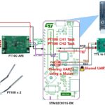
Part 2: Reading PT100 Signals Using STM32F103 ADC (Polling Method)
Reading PT100 Signals with STM32F103 ADC (Polling Method Experiment)
Part 3: STM32 ADC Time-Distributed Sampling Design Method
STM32 ADC Time-Distributed Sampling Design Method
Part 4: Implementing PT100 Temperature Measurement Using STM32 ADC DMA
Implementing PT100 Temperature Measurement Using STM32 ADC DMA
Part 5: 3-Wire PT100 Constant Current Driven AFE Design (TLV9062 + INA826)


“3-Wire PT100 Constant Current Driven AFE Design(TLV9062+INA826)”에 대한 4개의 생각