Introduction
When studying electronics and working in the electronics field, you eventually encounter a wide range of technologies.
From hardware design to software (firmware) coding, and even automation machinery, there are many areas to explore.
Of course, it is impossible to master everything, but developers naturally continue expanding their knowledge step by step.
This time, I decided to explore FPGA, an area closely related to semiconductor design, for the first time.
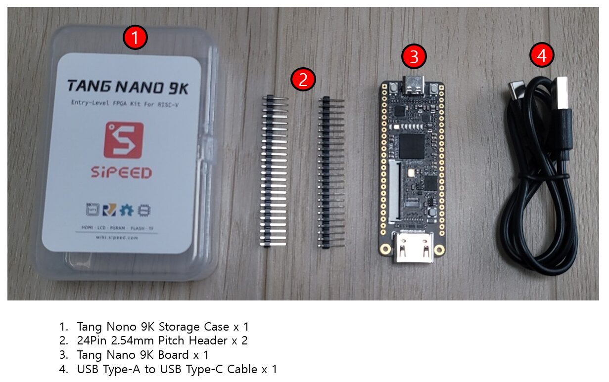
Recently, I purchased the Tang Nano 9K board by Sipeed
and went through the entire process from unboxing and development environment setup
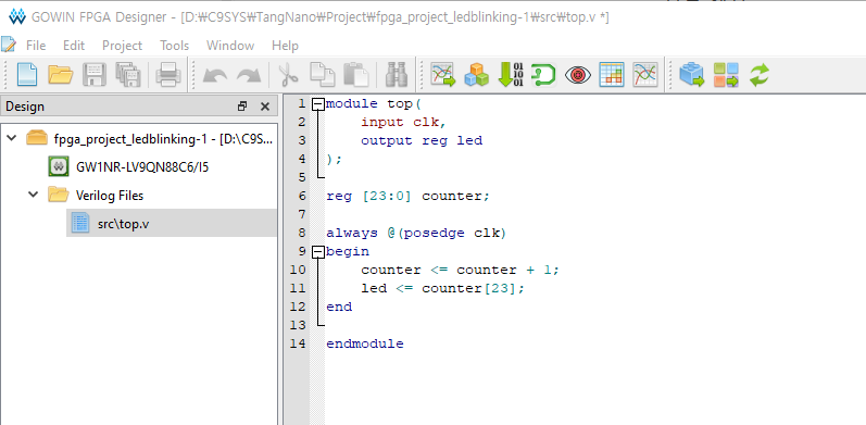
to running the most basic LED Blink test.
This article is both a beginner’s FPGA learning record and a practical hands-on experiment log.
Why Start Learning FPGA?
Why I Decided to Learn FPGA
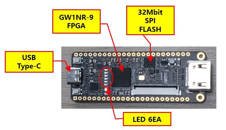
Although the Tang Nano 9K is designed as an entry-level board, it includes most of the essential features needed for FPGA learning.
In particular, features such as user LEDs, SPI Flash, PLL, and GPIO are provided by default, making the board suitable not only for simple LED blink tests but also for expanding into experiments involving UART, SPI, and PWM.
Another major advantage for beginners is that development can be done using only a USB connection without requiring a separate external download/programming device.
From the perspective of someone learning FPGA for the first time, I think this scale of device is more suitable for understanding the structure and practicing development than starting immediately with a very large FPGA.
More detailed information can be found on the Sipeed Wiki page.
Tang Nano 9K Sipeed Wiki
Development Environment Setup
Installing Gowin EDA
To use the Tang Nano 9K, the first step is to install the FPGA development tools.
Since the Tang Nano 9K uses a FPGA from Gowin Semiconductor, the official development environment, Gowin EDA, must be used.
Gowin EDA is an integrated development environment that supports synthesizing HDL code written in Verilog or VHDL, performing Place & Route, and downloading the resulting design into the FPGA.
Gowin EDA can be downloaded from the official GOWIN EDA Home page.
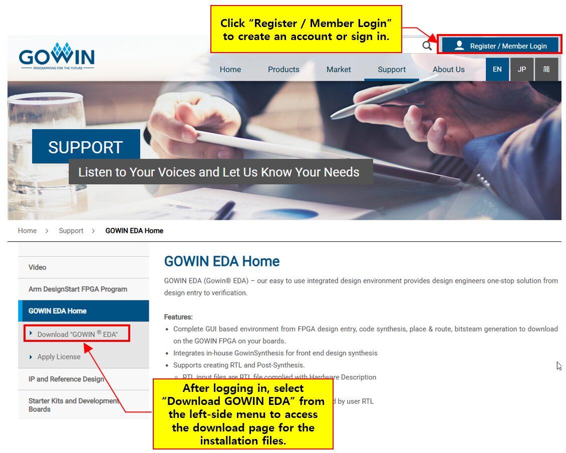
If this is your first visit, you will need to create an account first by selecting Register.
After signing up and logging in, the installation files can be downloaded from the Gowin EDA page under the Support menu.
As shown in the figure below, after clicking “Register / Member Login” and signing in, select the “Download GOWIN EDA” item from the left-side menu to download the installer.
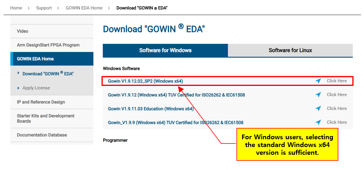
The software is available in both Windows and Linux versions, so you can simply choose the version that matches your operating system.
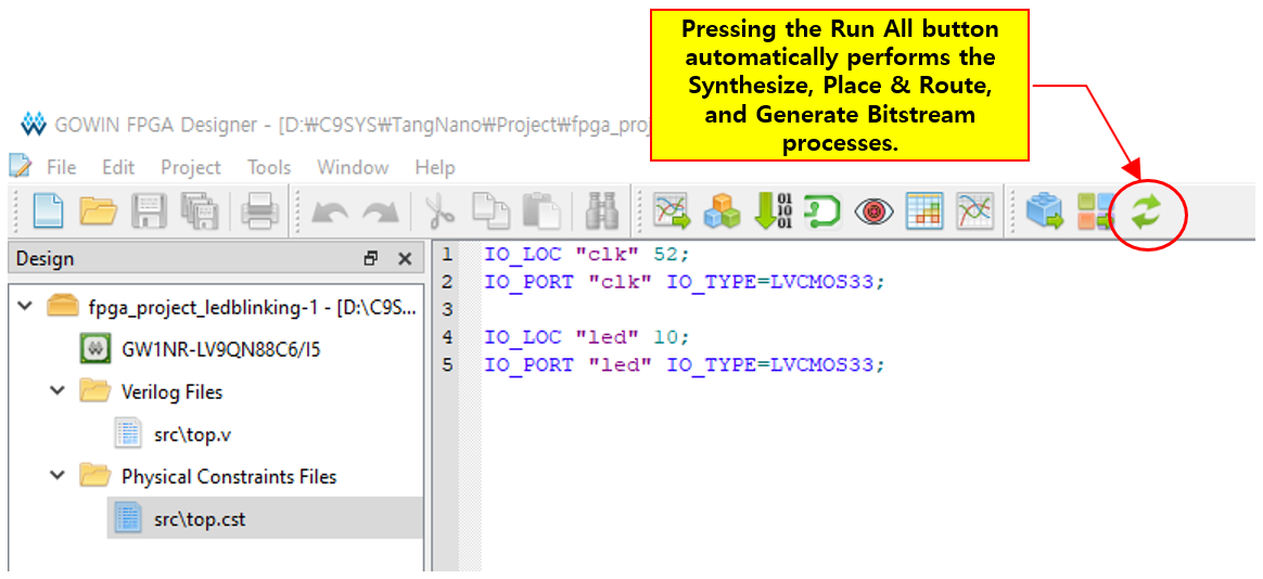
Writing the Constraint File
In FPGA development, the actual pin connections are not determined by Verilog code alone.
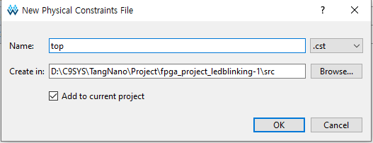
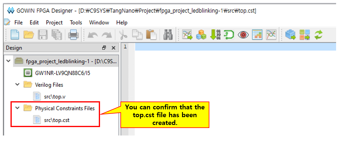
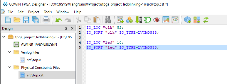
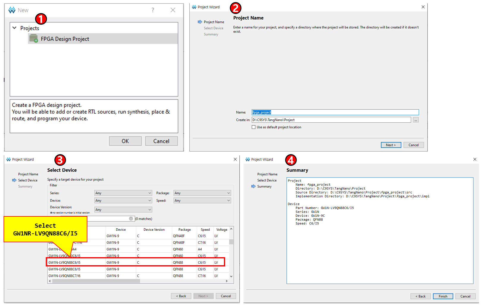
Therefore, a Constraint file must be created to connect the clk and led signals to the real FPGA pins.
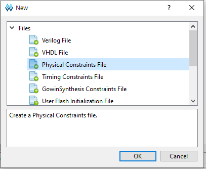
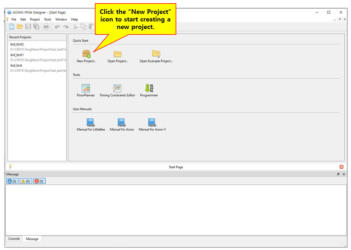
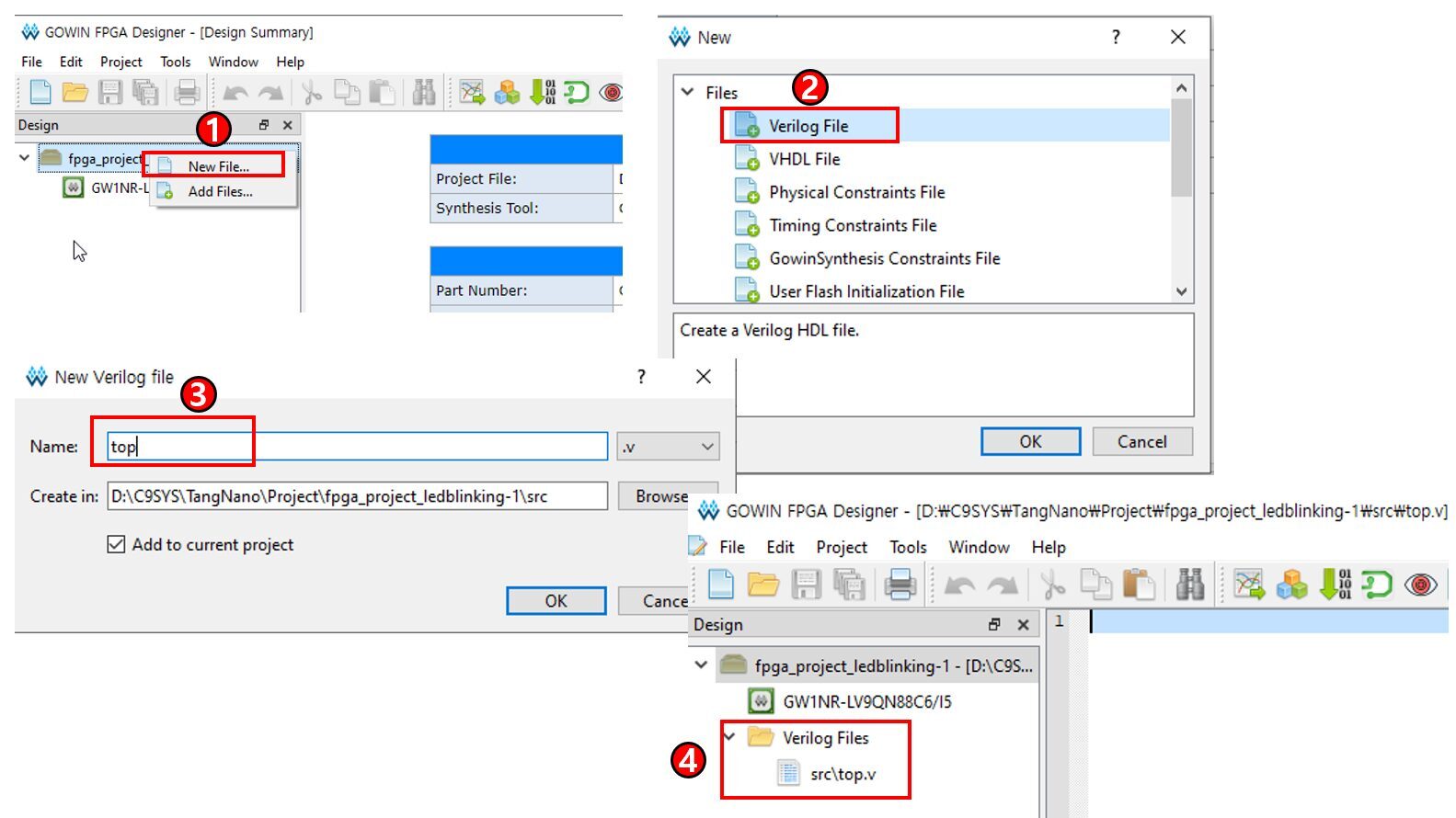
First, right-click inside the project window and select New File.
Then select Physical Constraints File as the file type to create the Constraint file.